
Gallium oxide (Ga2O3) is an ultrawide-bandgap oxide semiconductor increasingly studied for high-voltage electronics, solar-blind ultraviolet detection, thin-film systems, sensing platforms and next-generation materials engineering. Its combination of a bandgap above 4.5 eV, high critical electric-field potential and access to melt-grown beta-phase single crystals has made it a focal material for laboratories and industrial development teams working beyond conventional silicon technologies.
Eata Energy supplies gallium oxide raw materials in formats suited to powder processing, ceramic preparation, physical vapor deposition, crystal and epitaxy studies, and device-oriented research.
Also known as gallium(III) oxide, gallium trioxide or gallium sesquioxide, Ga2O3 occurs in several polymorphs. The monoclinic beta phase is the thermodynamically stable form, while alpha, gamma, delta and epsilon-related phases are generally treated as metastable structures. The phase, purity and processing history can influence optical, electrical and microstructural behavior, so the intended experiment or manufacturing route should guide material selection.
| Property | General Information |
| Chemical name | Gallium(III) oxide / gallium sesquioxide |
| Chemical formula | Ga2O3 |
| CAS Registry Number | 12024-21-4 |
| Molecular weight | 187.44 g/mol |
| Common appearance | White to off-white fine powder; crystalline forms are also available |
| Stable polymorph | Beta-Ga2O3, monoclinic |
| Other reported polymorphs | Alpha, gamma, delta and epsilon / kappa-related phases |
| Key material class | Ultrawide-bandgap oxide semiconductor |
| Common purity inquiries | 99.9% (3N), 99.99% (4N), 99.999% (5N), subject to form |
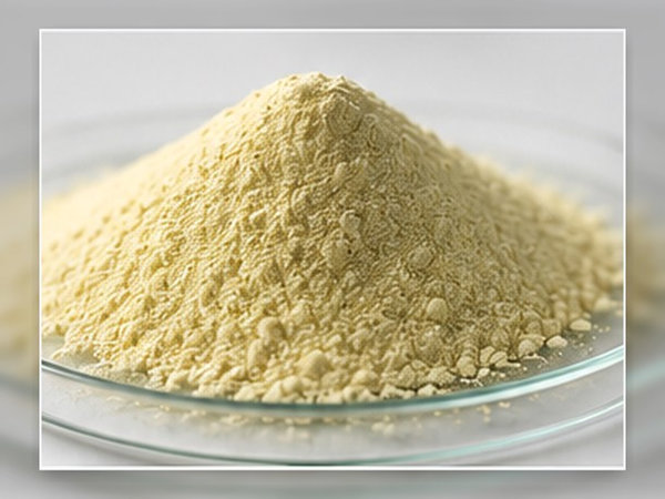 Fig. 1. Illustrative high-purity gallium oxide powder prepared for advanced materials processing.
The strongest interest in gallium oxide comes from its role as an ultrawide-bandgap semiconductor. Beta-Ga2O3 is widely discussed for power switching because its large bandgap is associated with a high theoretical breakdown field. It can also be grown as a bulk crystal from the melt, providing native substrates for homoepitaxy and device research - an important distinction from several other emerging oxide semiconductors.
Its optical absorption edge also supports solar-blind ultraviolet research, where a detector is designed to respond to deep-UV radiation while rejecting most visible and solar background light. Beyond electronic devices, Ga2O3 powders, films and nanostructures are investigated in gas sensing, photocatalysis, transparent or functional coatings, high-temperature monitoring and heterogeneous material systems.
| Product Form | Typical Inquiry Options | Common Uses |
| High-Purity Gallium Oxide Powder | 3N, 4N or 5N purity; beta phase or phase-defined material; micron-scale or fine powder | Ceramic processing, solid-state synthesis, target fabrication, catalyst and sensor research |
| Beta-Ga2O3 Powder | Monoclinic beta phase; controlled purity, particle size and morphology | Semiconductor materials studies, sintering, precursor development and phase-controlled experiments |
| Gallium Oxide Nanopowder / Fine Powder | Nanoscale or submicron particle ranges, surface-area and agglomeration requirements | Nanostructure synthesis, gas sensing, photocatalysis, inks, coatings and composite research |
| Ga2O3 Sputtering Target | Planar target, bonded or unbonded; round, rectangular or custom geometry; target density and backing plate options | RF sputtering, oxide thin films, optical coatings, electronic and sensor layers |
| Rotatable Gallium Oxide Target | Cylindrical target format, purity and composition tailored to compatible coating systems | Large-area coating development and extended sputtering campaigns |
| Beta-Ga2O3 Single Crystal Substrate | Undoped, Sn-doped or Fe-doped options; orientations may include (001), (010), (011), (-201), (100) and (110) | Homoepitaxy, Schottky diodes, FET research, UV photodetectors and crystallographic studies |
| Gallium Oxide Crystal / Wafer Pieces | Orientation, thickness, surface finish, dimensions, resistivity or dopant condition | Small-area device trials, spectroscopy, polishing studies and process development |
| Gallium Oxide Ceramic Shapes | Plates, rods, pressed forms or custom sintered geometries, subject to feasibility | Source material, process fixtures, ceramic development and specialized deposition studies |
| Doped or Composition-Adjusted Ga2O3 | Donor or compensating dopants, target composition and analytical limits defined by project | Conductivity control, insulating substrates, defect studies and comparative device research |
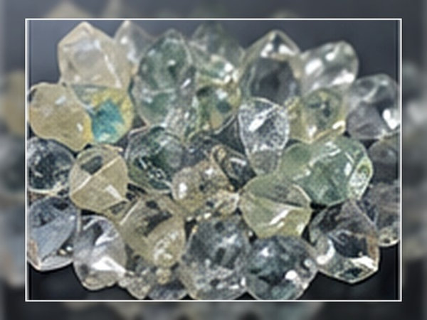 Fig. 2. Representative crystalline gallium oxide material for phase, morphology and optical studies.
Choosing Ga2O3 by name alone is not enough. Powder intended for sintering is evaluated differently from a sputtering target, and a substrate for epitaxy requires information that is irrelevant to a catalyst study.
| Project Direction | Information to Include in the Inquiry |
| Powder synthesis or ceramic development | Specify purity, beta-phase content, particle size distribution, morphology, moisture expectations and batch quantity. |
| Thin-film deposition by sputtering | Define target dimensions, thickness, density, purity, bonding method, backing plate, allowable porosity and compatible power conditions. |
| Single-crystal or epitaxy research | Confirm orientation, miscut, dimensions, thickness, doping, conductivity or resistivity, polish side, surface roughness and edge treatment. |
| Nanomaterial and sensor studies | Discuss primary particle size, agglomeration, surface area, dispersion behavior and whether a powder or dispersion is preferred. |
| Optical or UV detector programs | Align phase, substrate orientation, film route, defect strategy and spectral objective before choosing a raw material format. |
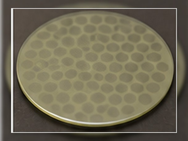 Fig. 3. Gallium oxide wafer concept for substrate selection, surface finishing and epitaxial development.
Beta-Ga2O3 is evaluated for Schottky barrier diodes, field-effect transistors and other high-voltage switching structures. Development work often examines breakdown behavior, leakage current, contact design, interface engineering, thermal management and the influence of crystal orientation. Its use is especially relevant to future power conversion systems where compact, high-field semiconductors could complement existing silicon, silicon carbide and gallium nitride platforms.
The deep-ultraviolet response of Ga2O3 supports solar-blind photodetector research for flame sensing, environmental monitoring, industrial process observation, electrical-discharge detection and high-temperature UV measurement. Material phase, oxygen vacancies, dopants, film quality and device architecture can strongly affect dark current, responsivity and response speed.
Gallium oxide sputtering targets and evaporation-oriented source materials can be used to explore dielectric, semiconducting and optical films. Researchers frequently investigate deposition power, oxygen partial pressure, substrate temperature and post-deposition annealing to control phase formation, transparency, conductivity and surface morphology.
Ga2O3 nanoparticles, nanowires and porous films are studied for chemical sensing and photocatalytic behavior. Fine powders are attractive when the project depends on surface area, defect chemistry or integration into composites. Particle size, agglomeration and thermal treatment should be specified because they can alter the resulting microstructure and response.
Single-crystal substrates support homoepitaxial and heterostructure investigations across MBE, MOCVD, HVPE, mist CVD, PLD, LPCVD and related routes. Orientation and doping are not secondary details: they influence growth kinetics, anisotropic transport, surface behavior, cleavage and device processing.
 Fig. 4. Conceptual Ga2O3 lattice image representing crystal structure and phase-dependent materials research.
Advanced materials purchasing works best when product naming, measurable specifications and the end process are connected. Eata Energy helps customers define a practical gallium oxide requirement instead of relying on a generic grade description.
 Fig. 5. Semiconductor device concept showing where gallium oxide films and substrates may support power and sensing research.
Not every project fits a catalogue specification. Eata Energy can discuss customized gallium oxide solutions based on chemical purity, polymorph, particle-size range, morphology, dopant, target shape, backing plate, substrate orientation, wafer dimensions, thickness, polishing condition, packaging and analytical requirements. Custom development begins with the customer's process and acceptance criteria, allowing the material format to be built around the intended use rather than forcing the project to adapt to a standard item.
Send us your target specification, drawing, equipment compatibility information or research objective. Our team will review the request and help identify a suitable Ga2O3 raw material route for evaluation.
| Catalog Number | Product Name | Order | Quantity |
|---|---|---|---|
| OACGO-0001 | Gallium Oxide, 99.999% (5N) | Inquiry | |
| OACGO-0002 | Ultra-High-Purity Gallium(III) Oxide Powder, 99.999% | Inquiry | |
| OACGO-0003 | 99.99% Gallium Oxide Ceramic Sputtering Target (Ga2O3), White, 6.44 g/cm3 | Inquiry | |
| OACGO-0004 | Gallium(III) Oxide, 99.99% Metals Basis | Inquiry | |
| OACGO-0005 | Gallium(III) Oxide, >=99.999% Metals Basis | Inquiry |
For Research or Industrial Raw Materials, Not For Personal Medical Use!
|
There is no product in your cart. |

Eata Energy is your trusted partner for high-performance energy materials, customized R&D support, and a stable global supply chain. We support you every step of the way in energy innovation.
Enter your E-mail and receive the latest news from us.
Copyright © Eata Energy. All rights reserved.
