
When Dmitri Mendeleev first sketched his periodic table in 1871, he left a deliberate gap beneath silicon, assigning it the provisional name "eka-silicon" and predicting its atomic weight, density, and chemical properties with uncanny precision. Fifteen years later, German chemist Clemens Winkler isolated this very element from the mineral argyrodite and named it germanium — the most celebrated vindication of Mendeleev's periodic law. Today, this lustrous gray-white metalloid — atomic number 32, diamond cubic crystal structure, a narrow bandgap of 0.67 eV — ranks among the most strategically critical materials on Earth, indispensable to thermal imaging systems, space-bound solar arrays, and the fiber optic networks that carry the world's data.
Eata Energy supplies high-purity germanium metal across grades from 4N (99.99%) to 6N (99.9999%), available as single-crystal and polycrystalline ingots, wafers, sputtering targets, powder, and precision optical blanks. Each batch undergoes rigorous characterization via GDMS and ICP-MS, with comprehensive analytical documentation provided to support your infrared optical, photovoltaic, semiconductor, or detector fabrication program.
Germanium's diamond cubic crystal structure — shared with silicon and diamond — endows it with a unique combination of semiconductor properties, high refractive index, and broad infrared transparency that no other element can replicate in a single material form.
| Property | Value | Notes |
| Atomic Number | 32 | Group 14, Period 4 |
| Atomic Weight | 72.63 g/mol | |
| Density | 5.323 g/cm³ | Diamond cubic |
| Melting Point | 938.25°C | |
| Boiling Point | 2833°C | |
| Bandgap | 0.67 eV | @ 300K, indirect |
| Refractive Index | 4.00 | @ 10 μm, highest of IR materials |
| IR Transmission | 2–14 μm | MWIR + LWIR windows |
| CAS Number | 7440-56-4 | EINECS: 231-164-3 |
| Crystal Structure | Diamond cubic | Like Si and diamond |
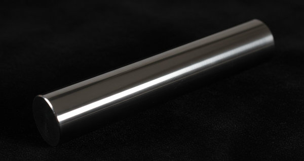 Figure 1: Zone-refined high-purity germanium crystal bar with characteristic dark silver-gray metallic luster
Germanium naturally occurs in five stable isotopes, with ⁷²Ge constituting approximately 27.7% of natural abundance. This isotope has attracted intense scientific interest as the target material in neutrinoless double-beta decay experiments, which seek to determine whether the neutrino is its own antiparticle — a discovery that would fundamentally reshape the Standard Model of particle physics.
Our germanium product range addresses the specific requirements of infrared optics, semiconductor epitaxy, radiation detection, and advanced research, with each form manufactured and packaged to preserve surface quality and crystallographic integrity.
Single-crystal and polycrystalline germanium ingots serve as feedstock for wafer slicing, optical blank fabrication, and crystal growth research. Material is produced via Czochralski or zone-refining methods depending on the target application and purity requirement.
Polished germanium wafers serve as substrates for III-V multijunction solar cell epitaxy, while optical blanks are fabricated into lenses, windows, prisms, and ATR crystals for infrared spectroscopy and thermal imaging systems.
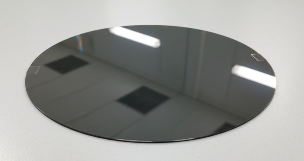 Figure 2: Polished germanium wafer with mirror-like surface and crystallographic orientation flats
HIP-consolidated germanium sputtering targets and zone-refined evaporation pellets support research into Ge-channel CMOS transistors, SiGe heterojunction bipolar transistors, and novel infrared thin-film coatings.
High-purity germanium powder serves as feedstock for alloy development, thermoelectric material synthesis, and research into germanium-based nanostructures including germanene — the two-dimensional topological insulator analog to graphene.
Germanium's defining optical property is its broad infrared transparency — transmitting wavelengths from 2 to 14 μm, encompassing both the mid-wave IR (MWIR, 3–5 μm) and long-wave IR (LWIR, 8–12 μm) atmospheric windows. With a refractive index of approximately 4.0 at 10 μm — the highest of any common IR optical material — germanium lenses achieve high numerical apertures in remarkably compact form factors, enabling miniaturized LWIR camera modules for automotive night vision, aerial thermography, firefighting thermal imagers, and military targeting systems. The strong Fresnel reflection losses at uncoated surfaces (~36% per surface) are mitigated by standard diamond-like carbon (DLC) and zinc sulfide anti-reflection coatings, achieving >95% transmission per surface in operational systems.
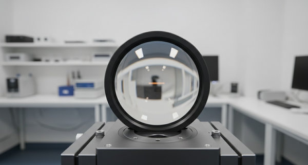 Figure 3: Precision-polished germanium plano-convex lens mounted on an optical test platform
Germanium substrates dominate the multijunction solar cell market for space applications, where efficiency takes precedence over cost. Single-crystal germanium wafers serve as the mechanical substrate and bottom-cell active layer for triple-junction GaInP₂/GaAs/Ge cells that have achieved efficiencies exceeding 47% under concentrated sunlight. The lattice constant of germanium (5.658 Å) provides excellent matching for III-V epitaxial growth, while its mechanical robustness withstands the extreme thermal cycling of orbital environments. Over 25 million 5G base stations expected by 2028 will drive demand for InP substrates grown from high-purity indium, while the concurrent expansion of low-earth-orbit satellite constellations continues to fuel germanium consumption for space photovoltaic systems.
Ultra-high-purity germanium (HPGe), achieved through multiple zone-refining passes, reaches net impurity concentrations below 10¹⁰ cm⁻³ — equivalent to one impurity atom per 10¹³ germanium atoms. When cooled to liquid nitrogen temperature (77 K), HPGe crystals function as the premier gamma-ray detectors in nuclear medicine, astrophysics, and homeland security applications. The superior energy resolution of HPGe detectors — typically 0.1–0.2% FWHM at 1.33 MeV — far exceeds that of scintillation-based alternatives, enabling precise isotope identification in complex gamma-ray spectra.
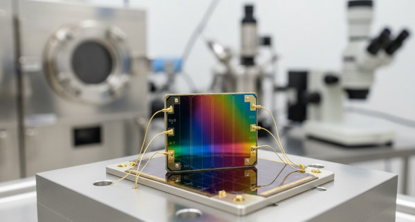 Figure 4: Multijunction solar cell on germanium substrate with gold wire bonds on test fixture
In the form of germanium tetrachloride (GeCl₄), germanium serves as the key dopant in silica optical fiber, raising the refractive index of the fiber core above the cladding to achieve total internal reflection. Essentially all single-mode fiber worldwide contains a germanium-doped silica core. The global rollout of 5G infrastructure, data center expansion, and fiber-to-the-home deployment continues to drive substantial germanium consumption in telecommunications — approximately 30% of global refinery output.
Silicon-germanium (SiGe) alloys have re-emerged as critical materials in high-frequency microelectronics, leveraging germanium's higher electron and hole mobilities compared with silicon to achieve cutoff frequencies above 500 GHz in heterojunction bipolar transistors. SiGe BiCMOS technology powers millimeter-wave radar, 5G/6G transceivers, and optical communication ICs. At the research frontier, epitaxial germanium channels are being integrated into CMOS architectures to extend Moore's Law, while monolayer germanene — the germanium analog of graphene — exhibits promise as a two-dimensional topological insulator for quantum computing applications.
 Figure 5: Illuminated fiber optic bundle with glowing tips transmitting data signals
Germanium purity selection directly influences device performance, detector energy resolution, and optical transmission characteristics. The matrix below provides practical guidance for grade selection.
| Grade | Characteristics | Recommended For |
| Ge 4N (99.99%) | Standard optical; metals < 100 ppm | General IR optics, fiber optic precursor, alloys |
| Ge 5N (99.999%) | Optical-grade; metals < 10 ppm | Thermal imaging lenses, solar cell substrates, ATR crystals |
| Ge 6N (99.9999%) | Semiconductor/detector-grade; ppb control | HPGe detectors, MBE source, SiGe epitaxy, research standards |
Eata Energy applies a rigorous multi-technique analytical protocol to certify every germanium batch, with results compiled in a Certificate of Analysis delivered with each shipment.
Frontier research in infrared optics, quantum devices, and next-generation photovoltaics frequently demands germanium configurations beyond standard catalog offerings. Eata Energy's technical team collaborates directly with your engineers to develop bespoke solutions.
Engage our materials scientists during your project scoping phase to optimize germanium grade, crystal orientation, and surface specification for your specific optical system, detector architecture, or epitaxial growth protocol.
| Catalog Number | Product Name | Order | Quantity |
|---|---|---|---|
| HPMHPR-0001 | 99.999% Germanium Ring (Ge) | Inquiry | |
| HPM-HGE-0001 | Ultra-High-Purity Germanium Microfoil on Aluminum Backing | Inquiry | |
| HPMHPR-0002 | 99.999% Germanium Sputtering Target (Ge) | Inquiry | |
| HPM-HGE-0002 | High-Purity Germanium Sputtering Target | Inquiry | |
| HPM-HGE-0003 | High-Purity Polycrystalline Germanium Rod | Inquiry | |
| HPM-HGE-0004 | High-Purity Germanium Single Crystal | Inquiry | |
| HPM-HGE-0005 | High-Purity Germanium Pellets and Lumps | Inquiry | |
| HPM-HGE-0006 | High-Purity Germanium Foil and Sheet | Inquiry | |
| HPM-HGE-0007 | High-Purity Germanium Disk, 1 mm Thick | Inquiry |
For Research or Industrial Raw Materials, Not For Personal Medical Use!
|
There is no product in your cart. |

Eata Energy is your trusted partner for high-performance energy materials, customized R&D support, and a stable global supply chain. We support you every step of the way in energy innovation.
Enter your E-mail and receive the latest news from us.
Copyright © Eata Energy. All rights reserved.
