
Organic photovoltaic materials enable thin, lightweight, and solution-processable solar devices built from semiconducting polymers and organic molecules. The active layer is commonly formed from an electron-donating material and an electron-accepting material, selected to combine complementary light absorption, suitable energy levels, efficient charge separation, balanced carrier transport, and a stable nanoscale morphology.
Eata Energy supplies materials for organic solar cell research, formulation development, coating trials, device optimization, and industrial materials evaluation.
The chemistry of an OPV material matters because every component contributes to the complete device rather than acting as an isolated absorber. Donor and acceptor materials must form interfaces where photo-generated excitons can dissociate, while their energy levels and transport characteristics must support movement of holes and electrons toward the appropriate contacts. Film morphology is equally important: domains that are too coarse can limit exciton harvesting, while excessive mixing can interrupt continuous transport pathways.
Modern organic solar cells include polymer-fullerene, polymer-non-fullerene, all-polymer, all-small-molecule, and multicomponent active layers. Non-fullerene acceptors have expanded the available absorption and energy-level design space, while established fullerene materials remain valuable for benchmark devices, morphology studies, ternary blends, and interface research. The most appropriate material system depends on the intended architecture, coating method, substrate, optical target, and stability program.
| Material Family | Representative Names | Typical Use in OPV Development |
| Conjugated polymer donors | P3HT; PTB7; PTB7-Th / PCE10; PCDTBT; PBDB-T / PCE12; PM6 / PBDB-T-2F; PM7; PTQ10; D18 / PCE18 | Photoactive electron-donor component, benchmark blends, visible and near-infrared absorption, solution-coated bulk heterojunction layers |
| Small-molecule donors | DRTB-T; DRCN5T; BTR-type donors; benzodithiophene- and oligothiophene-based donor molecules | All-small-molecule devices, ternary formulations, controlled molecular identity, complementary absorption and morphology tuning |
| Fullerene acceptors | PC61BM / PC60BM; PC71BM / PC70BM; ICBA and related soluble fullerene derivatives | Benchmark electron acceptors, polymer-fullerene devices, ternary blends, electron-transport and interfacial studies |
| Non-fullerene acceptors | ITIC; ITIC-2F; ITIC-4F / IT-4F; ITIC-Th; IDIC derivatives; Y6 / BTP-4F; Y7 / BTP-4Cl; N3; IEICO-4F | Broad and tunable optical absorption, low-band-gap active layers, high-performance polymer-NFA systems, near-infrared response |
| Polymer acceptors | N2200 / PNDI(2OD)2T; n-type conjugated polymers; all-polymer solar cell acceptors | All-polymer active layers, mechanical flexibility studies, charge-transport and morphology control |
| Interface and transport materials | PEDOT:PSS; PFN-Br; PEIE; PDIN; PDINN; BCP; selected hole- and electron-selective interlayers | Work-function adjustment, charge extraction, contact selectivity, reduced interfacial recombination, inverted and conventional device structures |
| Morphology and formulation components | Ternary modifiers, nucleating agents, compatible processing additives, crosslinkable components, host polymers and selected solvent systems | Blend morphology control, coating-window development, film uniformity, stability screening and process translation |
 Figure 1. Flexible organic photovoltaic films demonstrate the format versatility of solution-processable semiconductor layers.
A successful donor-acceptor combination is defined by more than a familiar material name. Absorption complementarity determines how effectively the blend uses the incident spectrum. Frontier energy levels influence charge transfer, open-circuit voltage, and contact selection. Molecular packing and miscibility affect domain formation, crystallinity, orientation, and the continuity of charge-transport pathways. Solubility and aggregation behavior determine whether the material can be processed reproducibly at the required concentration and coating speed.
For polymer donors, molecular weight distribution, dispersity, backbone regularity, end groups, residual catalyst, and batch-to-batch consistency can alter solution behavior and film morphology. For small molecules and non-fullerene acceptors, identity, isomer composition, purity, thermal transitions, optical absorption, and solid-state packing are common evaluation points. Fullerene derivatives are often compared by purity, solubility, aggregation behavior, and the reproducibility of benchmark blends.
| Example Pairing | Why It Is Commonly Studied | Information to Confirm |
| P3HT : PC61BM | Widely used benchmark system for process, morphology, degradation, and device-physics studies | P3HT molecular weight and regioregularity; PC61BM purity; solvent; ratio; annealing method |
| PTB7 or PTB7-Th : PC71BM | Low-band-gap polymer-fullerene platform with extended absorption and extensive literature history | Polymer batch data; fullerene grade; additive use; active-layer thickness; interface materials |
| PBDB-T : ITIC or related ITIC derivative | Established non-fullerene platform for energy-level and morphology comparison | Exact acceptor derivative; donor molecular weight; blend ratio; thermal and solvent treatment |
| PM6 : Y6 or Y6-family acceptor | Representative modern polymer-NFA pairing used in high-performance device research | PM6 batch specification; Y-series identity; purity; concentration; processing solvent; film-treatment conditions |
| D18 : Y6-family acceptor | Narrow-band-gap donor platform used for advanced binary and ternary device studies | Donor molecular weight; acceptor side-chain variant; ratio; morphology-control strategy |
| Donor polymer : N2200-type polymer acceptor | All-polymer active layer for mechanical, morphology, and stability research | Both polymer molecular-weight distributions; miscibility; solvent system; coating temperature |
These combinations are presented as recognizable research references and search terms, not as universal formulations. Device results depend strongly on material batch, purification, layer sequence, substrate preparation, atmosphere, coating protocol, thickness, post-treatment, and measurement method.
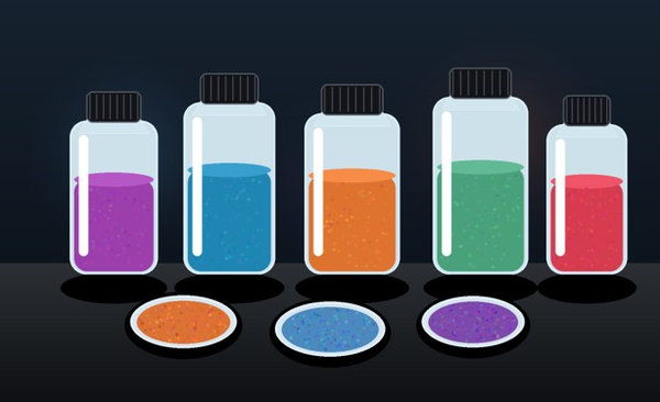 Figure 2. Donor polymers and acceptor molecules can be supplied as high-purity solids or project-defined formulations.
A useful product specification should connect chemical identity with the parameters that affect solution preparation, thin-film formation, and device comparison. The appropriate test package varies by material class, and not every parameter is available for every item. Eata Energy can organize product discussions around the following categories so that critical acceptance criteria are identified early.
| Selection Parameter | Why It Matters | Examples of Requested Information |
| Chemical identity and structure | Avoids confusion between derivatives, side-chain variants, salts, isomers, or similarly named polymers | Full chemical name, repeat-unit description, CAS number where applicable, structure or literature reference |
| Purity and impurity profile | Trace impurities, residual monomer, catalyst, or side products may influence recombination, stability, and film formation | HPLC or NMR purity, residual metals, elemental data, ash, moisture, selected impurity limits |
| Polymer molecular characteristics | Molecular weight and dispersity influence viscosity, aggregation, crystallization, and morphology | Mn, Mw, dispersity, GPC method and calibration basis, regioregularity, end-group information |
| Optical properties | Absorption profile and optical band gap help define spectral complementarity and thickness strategy | UV-Vis spectrum in solution or film, absorption maximum, onset, extinction information where available |
| Electronic properties | Energy levels guide donor-acceptor matching and contact selection | HOMO/LUMO or ionization energy/electron affinity, cyclic voltammetry method, reference electrode and calculation basis |
| Thermal behavior | Thermal transitions can affect drying, annealing, storage, and morphology evolution | TGA, DSC, melting or glass-transition information, decomposition behavior where available |
| Solubility and processing behavior | Affects formulation concentration, filtration, coating uniformity, and solvent selection | Compatible solvents, concentration range, dissolution temperature, aggregation tendency, filtration recommendation |
| Physical form and packaging | Controls handling, contamination risk, and suitability for solution preparation | Powder, crystal, pellet, concentrate, pre-formulated solution, package size, light or moisture protection |
| Batch-specific documentation | Supports comparison between screening, optimization, and larger development programs | Certificate of analysis, chromatogram, spectrum, GPC trace, NMR, MS, elemental analysis or project-specific data |
Organic photovoltaic layers are often deposited from solution by spin coating, blade coating, slot-die coating, bar coating, spray coating, gravure, flexographic, or inkjet-related methods. A material that performs well in a small spin-coated device may need a different concentration, solvent blend, drying profile, or additive strategy when transferred to a larger or faster coating process. The specification therefore needs to reflect the processing route as well as the molecular identity.
Important formulation variables include solids content, donor-to-acceptor ratio, viscosity, temperature, dissolution sequence, filtration, solvent volatility, substrate surface energy, wet-film thickness, drying rate, thermal or solvent-vapor treatment, and the compatibility of the active layer with adjacent interfaces. For scale-up-oriented work, customers may also evaluate coating uniformity, pinhole formation, edge behavior, residual solvent, batch aging, solution stability, and the sensitivity of film morphology to small process changes.
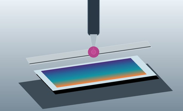 Figure 3. Controlled liquid formulation and coating conditions are central to uniform OPV active-layer formation.
The active layer must operate between selective contacts that extract one carrier while blocking the other. Organic and hybrid interfacial materials are used to modify work function, improve wetting, reduce recombination, protect the active layer, and support conventional or inverted architectures. Common research terms include PEDOT:PSS, PFN-Br, PEIE, PDIN, PDINN, BCP, conjugated polyelectrolytes, self-assembled interlayers, and crosslinkable contact modifiers.
Interface selection should consider the transparent electrode, metal electrode, active-layer surface, processing solvent, deposition sequence, thermal budget, and environmental sensitivity. A solvent that is suitable for one layer may dissolve or swell the layer beneath it. Likewise, an interlayer that provides a favorable work function can still fail if it forms an incomplete film, reacts with the active layer, or changes during storage. For this reason, device-stack information is valuable when sourcing both the photoactive materials and the supporting interlayers.
| Layer Function | Representative Material Types | Key Compatibility Questions |
| Transparent electrode interface | Conductive polymers, self-assembled modifiers, metal-oxide dispersions, surface-treatment materials | Does the layer wet the electrode, provide the required work function, and tolerate the next coating solvent? |
| Hole-selective layer | PEDOT:PSS grades, conjugated polyelectrolytes, organic hole-transport materials, selected oxides | Is the layer acidic or hygroscopic, and how does it affect active-layer stability and adhesion? |
| Photoactive layer | Polymer donor plus fullerene or non-fullerene acceptor; all-polymer or all-small-molecule blend | Are absorption, energy levels, mobility, miscibility, morphology, thickness, and processing window aligned? |
| Electron-selective layer | PFN-Br, PEIE, PDIN/PDINN families, BCP and related electron-transport or dipole-forming materials | Can it be deposited orthogonally, form a complete ultrathin film, and remain stable under the top electrode? |
| Top electrode and protection | Metal evaporation materials, conductive coatings, buffer layers, barrier and encapsulation materials | Does the deposition process damage the organic layers, and is the finished stack protected from oxygen, moisture, heat, and light? |
 Figure 4. OPV performance depends on the coordinated design of electrodes, transport layers, and the donor-acceptor active layer.
Organic photovoltaic materials are evaluated wherever low weight, mechanical compliance, tunable color, semitransparency, or solution-based manufacturing offers a useful design route. The material system and device construction should be selected for the actual operating environment rather than from efficiency data alone.
| Application Area | Material and Device Priorities |
| Flexible and lightweight solar devices | Low-temperature processing, bend tolerance, thin substrates, compatible electrodes, robust interfaces and encapsulation |
| Semitransparent photovoltaic glazing | Controlled visible transmission, color neutrality or intentional color, near-infrared harvesting, transparent contacts and optical-stack design |
| Indoor and low-light energy harvesting | Absorption matched to artificial lighting, low leakage, suitable voltage output, small-area module integration and long-duration stability |
| Wearable and portable electronics | Mechanical compliance, thin form factor, repeated bending, low mass, safe integration and barrier protection |
| Building-integrated photovoltaics | Large-area coating, appearance, module interconnection, outdoor stability, substrate compatibility and scalable materials supply |
| Agrivoltaic and greenhouse concepts | Spectral selectivity, transmission of plant-relevant wavelengths, environmental durability and large-area transparent module design |
| Sensors, photodetectors and energy-harvesting research | Narrow- or broad-band absorption, dark-current control, interfacial selectivity, response speed and custom spectral targets |
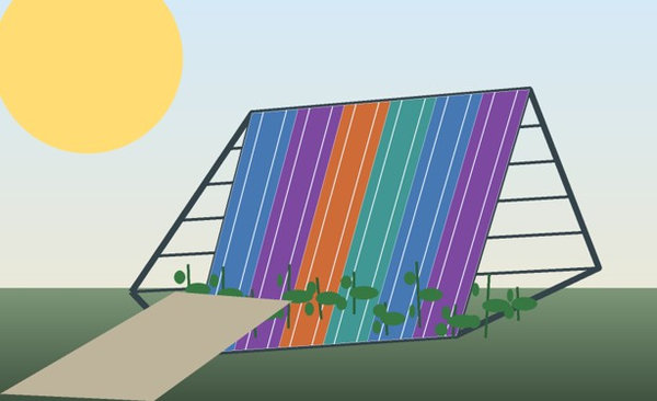 Figure 5. Semitransparent organic photovoltaic panels can be engineered for architectural and greenhouse light-management concepts.
| Eata Energy Capability | Value for Your Program |
| Application-led material selection | We review the intended device structure, layer function, processing route, and performance target before defining the most useful product specification. |
| Broad donor and acceptor vocabulary | Inquiries can cover established benchmark materials, modern non-fullerene systems, polymer acceptors, small molecules, and related interface materials. |
| Specification-focused communication | Identity, purity, molecular weight, optical properties, solubility, physical form, and available analytical data are discussed for the selected material rather than assumed from a generic name. |
| Support for comparative screening | Related donor grades, acceptor derivatives, molecular-weight ranges, or formulation options can be evaluated for controlled materials comparison. |
| Multiple supply formats | Depending on the product, materials may be considered as powders, crystals, polymer solids, dispersions, concentrates, or project-defined solutions. |
| Continuity from laboratory evaluation to larger programs | The same critical material attributes can be carried into scale-up discussions, with attention to batch definition, documentation, packaging, and change control. |
| Custom synthesis and formulation capability | Eata Energy can evaluate new structures, modified analogues, target molecular-weight ranges, purification requirements, solvent systems, concentrations, filtration, and device-specific formulations. |
Standard materials are effective for reproducing published devices and establishing internal benchmarks, but many programs require a modified structure, tighter impurity control, a different polymer molecular-weight range, improved solubility, a selected absorption band, or a formulation adapted to a specific coating method. Eata Energy can review custom requests for donor polymers, small-molecule donors, fullerene derivatives, non-fullerene acceptors, polymer acceptors, interfacial molecules, morphology-control components, and pre-formulated active-layer solutions.
Customization may include monomer or molecular structure selection; side-chain, end-group, or halogen substitution; target molecular weight and dispersity; regioregularity; isomer control; purification and residual-metal limits; optical or electrochemical targets; solvent exchange; concentration; donor-acceptor ratio; ternary-component addition; filtration; package format; and project-specific analytical documentation. Feasibility and acceptance criteria are defined for the individual project, so a chemical structure, publication, target specification, or device-development brief should be provided wherever possible.
| Catalog Number | Product Name | Order | Quantity |
|---|---|---|---|
| SEMOPM-0001 | C60MC12 Fullerene Semiconductor, ≥97% (HPLC) | Inquiry | |
| SEMOPM-0002 | PC61BM Fullerene Acceptor, ≥99% | Inquiry | |
| SEMOPM-0003 | ICBA Indene-C60 Bisadduct, >98.5% (HPLC), Isomer Mixture | Inquiry | |
| SEMOPM-0004 | Perylenetetracarboxylic Diimide (PTCDI), ≥95% | Inquiry | |
| SEMOPM-0005 | PC71BM Fullerene Acceptor, ≥97%, BHT-Stabilized | Inquiry | |
| SEMOPM-0006 | F4TCNQ Organic Semiconductor Dopant, ≥97% | Inquiry | |
| SEMOPM-0007 | Fullerene C70 Electron Acceptor, ≥99% | Inquiry | |
| SEMOPM-0008 | Fullerene C60, ≥99.0% (HPLC) | Inquiry | |
| SEMOPM-0009 | H101 EDOT-Based Hole-Transport Material, ≥95% | Inquiry | |
| SEMOPM-0010 | Perfluorinated Copper Phthalocyanine (F16CuPc), ≥80% | Inquiry |
For Research or Industrial Raw Materials, Not For Personal Medical Use!
|
There is no product in your cart. |

Eata Energy is your trusted partner for high-performance energy materials, customized R&D support, and a stable global supply chain. We support you every step of the way in energy innovation.
Enter your E-mail and receive the latest news from us.
Copyright © Eata Energy. All rights reserved.
