
Eata Energy supplies monocrystalline silicon for customers who need a controlled single-crystal structure, dependable electrical behavior, and project-specific material specifications. Our supply scope can cover monocrystalline silicon wafers, single-crystal silicon ingots, cut blocks, rods, pieces, and custom substrates for photovoltaic development, semiconductor research, power-device projects, sensors, precision processing, and advanced materials work.
Unlike multicrystalline material, monocrystalline silicon is formed as one continuous crystal lattice. This uniform structure supports predictable processing and makes the material a preferred platform where crystal orientation, conductivity type, resistivity, surface condition, and dimensional control matter. Eata Energy helps buyers match these variables to the intended process rather than treating every silicon grade as interchangeable.
Monocrystalline silicon, also called single-crystal silicon or mono-Si, has an ordered atomic arrangement extending through the material. The absence of grain boundaries distinguishes it from multicrystalline silicon and gives engineers a consistent base for doping, oxidation, diffusion, deposition, etching, texturing, lithography, and other downstream steps. The material can be selected by growth method and processed into circular wafers, pseudo-square photovoltaic wafers, cylindrical ingots, blocks, rods, or customer-defined geometries.
For solar and energy-related projects, monocrystalline silicon wafers provide a widely used platform for high-performance cell architectures. In electronics and laboratory development, polished or etched silicon wafers provide a controlled substrate for device fabrication, thin-film growth, microfabrication, and materials characterization. High-resistivity float-zone silicon is also relevant where low oxygen content, long carrier lifetime, or specialized electrical and optical behavior is required.
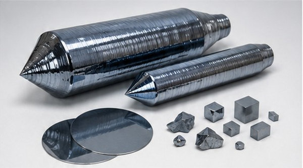 Figure 1. Representative single-crystal silicon ingots, wafers, and cut pieces.
| Product Form | Typical Use | Key Parameters to Define |
| Monocrystalline silicon ingots / boules | Cylindrical single-crystal material for wafering, machining, process development, or further conversion. | Growth method, diameter, conductivity type, dopant, resistivity, orientation, oxygen level, and usable length. |
| Monocrystalline silicon wafers | As-cut, lapped, etched, polished, or other application-specific surface conditions. | Diameter or side length, thickness, orientation, resistivity, flat/notch configuration, surface finish, TTV, bow, warp, and edge profile. |
| Photovoltaic mono-Si wafers | P-type or n-type wafers for solar-cell research, pilot processing, and industrial development. | Wafer format, conductivity type, thickness, resistivity, lifetime expectations, surface condition, and dimensional tolerances. |
| High-resistivity float-zone silicon | Low-oxygen single-crystal silicon for detectors, power devices, RF, optics, and demanding laboratory work. | Resistivity range, diameter, orientation, thickness, minority-carrier lifetime, and impurity requirements. |
| Blocks, rods, chunks, and cut pieces | Bulk forms for machining trials, materials research, target preparation, or custom component fabrication. | Shape, dimensions, mass, cut quality, crystal orientation, and surface treatment. |
| Custom silicon substrates and components | Round, square, rectangular, diced, or project-specific geometries. | Drawing, dimensional tolerance, surface roughness, edge treatment, cleaning, packaging, and inspection data. |
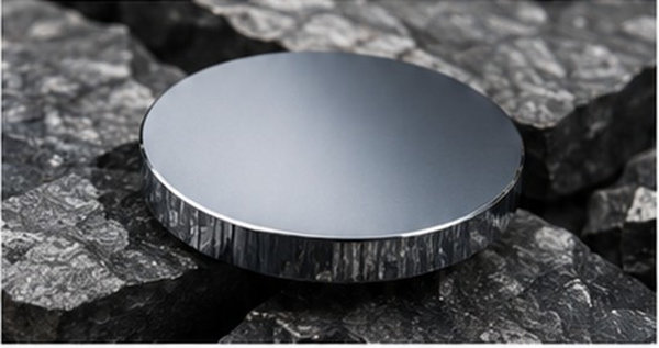 Figure 2. Polished monocrystalline silicon wafer prepared for precision processing.
| Parameter | Available Selection / Quotation Basis |
| Crystal structure | Single-crystal silicon with diamond-cubic structure |
| Growth method | Czochralski (CZ), float zone (FZ), or another agreed route |
| Conductivity type | P-type, n-type, or undoped / intrinsic where technically available |
| Common dopants | Boron, phosphorus, arsenic, or antimony depending on grade and application |
| Crystal orientation | (100), (111), or customer-specified orientation and off-angle |
| Resistivity | Specified by the customer for the intended electrical or device process |
| Product geometry | Wafer, ingot, boule, rod, block, piece, or custom-cut substrate |
| Surface condition | As-cut, lapped, etched, polished, single-side polished, double-side polished, or custom |
| Dimensions | Diameter, side length, thickness, length, and tolerances by inquiry or drawing |
| Geometric controls | TTV, bow, warp, flatness, edge profile, flat or notch, where applicable |
| Purity and impurities | Grade-dependent limits for oxygen, carbon, metals, and other controlled impurities |
| Inspection and documentation | Dimensional report, orientation, resistivity, surface data, or certificate options as agreed |
| Packaging | Protective wafer boxes, clean packaging, vacuum or inert packaging, or project-specific protection |
| Property | Reference Value |
| Density | 2.328 g/cm3 |
| Energy bandgap | 1.1242 eV |
| Lattice constant | 0.543095 nm |
| Melting point | 1415 deg C |
| Thermal conductivity | 150 W/m.K |
| Thermal expansion coefficient | 2.6 x 10^-6 K^-1 |
| Relative permittivity | 11.7 |
Reference values describe elemental silicon under standard reference conditions and should not replace a product-specific certificate or engineering review.
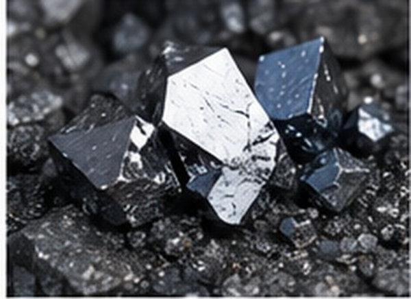 Figure 3. High-purity silicon pieces for material evaluation and specialized fabrication.
Czochralski (CZ) silicon. In the CZ process, a seed crystal is drawn from molten silicon held in a quartz crucible. This method is widely used for commercial single-crystal substrates and supports broad diameter and production options. Because the melt contacts a quartz crucible, oxygen can be incorporated into the crystal. The acceptable oxygen level depends on the device, thermal process, dopant system, and performance target.
Float-zone (FZ) silicon. The FZ route moves a localized molten zone along a silicon rod without a crucible. Impurities tend to remain in the molten region as the purified crystal solidifies behind it. FZ silicon is therefore selected for applications that value very low oxygen, high purity, high resistivity, long carrier lifetime, or specialized optical and detector performance. Diameter availability and cost can differ from CZ material, so the choice should be driven by the application rather than by a generic preference for one process.
Modified CZ, magnetic CZ, neutron-transmutation-doped material, epitaxial structures, and silicon-on-insulator configurations may also be relevant to specific projects. These are specialized requirements and should be stated clearly at the inquiry stage.
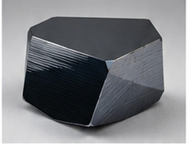 Figure 4. Custom-cut single-crystal silicon block for machining or substrate preparation.
Photovoltaic development: Mono-Si wafers for cell architecture research, passivation studies, diffusion and implantation trials, metallization development, texturing, coating evaluation, and pilot production.
Semiconductor and power devices: Substrates for diodes, transistors, integrated devices, power components, process qualification, and materials compatibility work.
MEMS and sensors: Single-crystal substrates for micromachining, pressure sensors, inertial structures, microfluidic components, and precision mechanical elements.
Optoelectronics and photonics: Silicon platforms for detectors, optical components, integrated photonics, infrared research, and high-resistivity electromagnetic applications.
Thin films and coatings: Controlled substrates for deposition, epitaxy, oxidation, dielectric stacks, metallization, adhesion studies, and interface characterization.
Laboratory and materials research: Wafers, pieces, and bulk samples for etching, doping, annealing, surface science, microscopy, spectroscopy, and device prototyping.
Custom industrial components: Machined or cut silicon shapes where thermal stability, crystal orientation, dimensional precision, or material compatibility is important.
| Decision Point | What to Specify |
| Start with the end process | Define whether the material will be wafered, oxidized, doped, etched, polished, machined, coated, or used as a bulk component. |
| Set conductivity and resistivity | Specify p-type, n-type, or undoped material and give the resistivity range that supports the device or experiment. |
| Confirm orientation | Select (100), (111), off-axis, or another orientation based on texturing, etching, cleavage, epitaxy, or device requirements. |
| Choose CZ or FZ intentionally | Use oxygen tolerance, resistivity, carrier lifetime, diameter, and process economics to guide the growth-method decision. |
| Define surface quality | State whether as-cut, etched, lapped, single-side polished, or double-side polished material is required. |
| Include geometry tolerances | Provide diameter or side length, thickness, TTV, bow, warp, edge profile, and drawing tolerances where these affect processing. |
| State impurity and documentation needs | Identify oxygen, carbon, metals, lifetime, inspection, traceability, cleaning, and packaging requirements before quotation. |
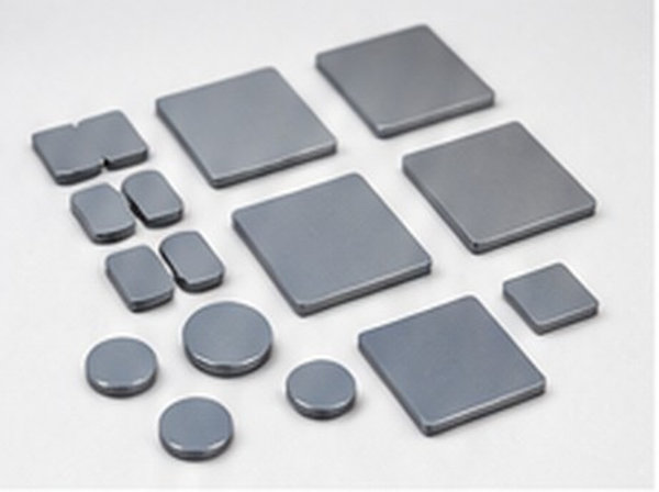 Figure 5. Assorted silicon substrate shapes for project-specific dimensions.
Eata Energy can coordinate custom monocrystalline silicon specifications for research programs, pilot processes, and industrial production needs. Customization may include material grade, CZ or FZ growth route, conductivity type, dopant, resistivity, crystal orientation, ingot or wafer dimensions, thickness, surface finish, edge condition, diced size, cut geometry, cleaning, packaging, and requested inspection data. Feasibility depends on the complete specification, so a drawing or parameter sheet is recommended for non-standard components.
For an accurate quotation, please include: product form, quantity, target dimensions, conductivity type, resistivity, orientation, growth method, purity or impurity limits, surface condition, tolerances, packaging needs, and the intended processing or application. This information allows the material selection to be aligned with the actual technical objective.
Discuss your monocrystalline silicon requirements with Eata Energy and request a specification-based quotation.
| Catalog Number | Product Name | Order | Quantity |
|---|---|---|---|
| SEM-MSS-0001 | Monocrystalline Silicon Wafer, P-type | Inquiry | |
| SEM-MSS-0002 | Ga-doped P-type Monocrystalline Silicon Wafer | Inquiry | |
| SEM-MSS-0003 | Monocrystalline Silicon Wafer, N-type | Inquiry | |
| SEM-MSS-0004 | Sb/P-doped N-type Monocrystalline Silicon Wafer | Inquiry | |
| SEM-MSS-0005 | Monocrystalline Silicon Wafer, N-type | Inquiry | |
| SEM-MSS-0006 | 3-inch N-type Lightly Doped Monocrystalline Silicon Wafers | Inquiry | |
| SEM-MSS-0007 | 4-inch N-type Lightly Doped Monocrystalline Silicon Wafers | Inquiry | |
| SEM-MSS-0008 | 3-inch Heavily Doped Monocrystalline Silicon Wafers | Inquiry | |
| SEM-MSS-0009 | 4-inch Heavily Doped Monocrystalline Silicon Wafers | Inquiry | |
| SEM-MSS-0010 | Monocrystalline Silicon Powder | Inquiry |
For Research or Industrial Raw Materials, Not For Personal Medical Use!
|
There is no product in your cart. |

Eata Energy is your trusted partner for high-performance energy materials, customized R&D support, and a stable global supply chain. We support you every step of the way in energy innovation.
Enter your E-mail and receive the latest news from us.
Copyright © Eata Energy. All rights reserved.
