
Quantum dot photoresist combines optically or electronically active quantum dots with a photosensitive matrix that can be patterned by controlled exposure and development. This format gives engineers a practical route to position quantum dots only where they are needed, creating defined pixels, microstructures, color-conversion regions, sensing elements, or other functional areas on a substrate.
Eata Energy supplies and develops quantum dot photoresist materials for customers working in advanced displays, micro-LED color conversion, photonic devices, optoelectronics, sensors, patterned coatings, and emerging energy-related research.
Conventional photoresists are optimized mainly to define a temporary or permanent pattern. A quantum dot photoresist must do more: it has to preserve nanocrystal dispersion and optical properties while also providing usable coating, exposure, development, adhesion, and curing behavior. A well-matched formulation can support direct patterning without the separate transfer steps often required for pre-deposited quantum dot films.
The interaction between quantum dots and the surrounding resin is especially important. Native ligands that stabilize colloidal nanocrystals may not be compatible with a polar photoresist matrix, and excessive ligand exchange, photoinitiator loading, ultraviolet exposure, heat, or developer contact can reduce photoluminescence or change the film morphology. For that reason, material selection should be based on the full process window rather than emission wavelength alone.
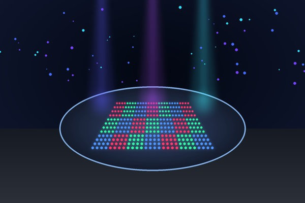 Figure 1. Conceptual optical exposure of a quantum-dot photoresist film to define addressable emissive regions on a wafer.
| Product | Typical Description | Potential Development Direction |
| Red-emitting quantum dot photoresist | Photosensitive formulation designed to create red-emissive or red color-conversion patterns. | Micro-LED color conversion, display pixels, optical markers, patterned luminescent films. |
| Green-emitting quantum dot photoresist | Photosensitive formulation for green-emissive or green color-conversion regions. | Microdisplays, pixelated converters, photonic structures, device prototyping. |
| Cadmium-free quantum dot photoresist | Formulation route based on cadmium-free quantum dot systems when compatible materials are required. | Display research, lighting, color conversion, and application-specific optical coatings. |
| InP-based QD photoresist | InP or related core/shell quantum dots incorporated into a patternable resin system, subject to project feasibility. | Visible-light color conversion, RGB pixel studies, micro-optical patterning. |
| Perovskite quantum dot photoresist | Photo-patternable or in-situ-forming perovskite quantum dot systems developed around their high absorption and narrow emission characteristics. | Microdisplay color conversion, photonic patterns, optoelectronic research. |
| QD/siloxane photo-patternable composite | Hybrid organic-inorganic matrices intended to improve dispersion, film integrity, or environmental resistance. | Color-conversion filters, thick patterned films, optical encapsulation concepts. |
| Direct-photopatternable QD formulation | Materials in which exposure changes solubility through polymerization, ligand crosslinking, additive crosslinking, or related photochemical routes. | High-resolution QD patterns, experimental QLED structures, integrated photonics. |
| Near-infrared quantum dot photoresist | Patternable formulation using NIR-active quantum dots when compatible with the selected photoresist chemistry. | Photodetector research, infrared sensing, spectral filters, patterned absorbers. |
| Custom QD-polymer photoresist | Application-specific mixture tuned around the selected quantum dot, binder, initiator, solvent, and development process. | Projects requiring non-standard emission, viscosity, film thickness, substrate compatibility, or optical density. |
Customers may also search for these materials using different technical names. Eata Energy can evaluate inquiries described as quantum dot color-conversion photoresist, QDPR, photopatternable quantum dot resin, red QD photoresist, green QD photoresist, cadmium-free QD photoresist, InP quantum dot photoresist, perovskite QD photoresist, micro-LED quantum dot photoresist, quantum dot color filter material, direct-photolithography QD formulation, or patterned quantum dot polymer composite.
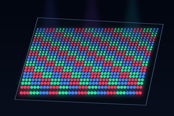 Figure 2. Dense red, green, and blue quantum-dot micro-pixels for color-conversion and high-resolution display development.
A useful quotation or technical comparison begins with the process conditions. Providing the items below helps narrow the formulation space and avoids selecting a material that is optically suitable but incompatible with the coating or lithography workflow.
| Selection Item | Information to Provide | Why It Matters |
| Quantum dot composition | Core, core/shell, alloyed, perovskite, carbon-based, or other requested system. | Defines the accessible spectral range, absorption, stability profile, and compatibility options. |
| Target emission or absorption | Peak wavelength, color coordinates, spectral width, excitation source, or NIR response. | Connects the material to the device optical design. |
| Photoluminescence requirements | Desired brightness, PLQY expectation, color purity, and allowable spectral shift after processing. | Evaluates whether the QD surface and matrix preserve optical output. |
| Quantum dot loading / optical density | Required solids content, QD concentration, blue-light absorption, or target conversion efficiency. | Balances optical performance against viscosity, aggregation risk, exposure depth, and resolution. |
| Resist tone and photochemistry | Negative-tone or positive-tone process; polymerization, crosslinking, ligand chemistry, or other imaging mechanism. | Determines which regions remain after development and how the QDs interact with exposure. |
| Exposure conditions | Exposure wavelength, tool type, dose window, mask or direct-write process, and atmosphere. | Guides photoinitiator selection and helps prevent insufficient cure or unnecessary optical damage. |
| Coating method | Spin coating, slot-die coating, blade coating, spray coating, ink dispensing, or another deposition method. | Sets practical requirements for viscosity, wetting, filtration, solids content, and drying behavior. |
| Film thickness and feature size | Target dry-film thickness, pixel dimensions, spacing, sidewall profile, and aspect ratio. | Thicker color-conversion layers may improve absorption, while finer patterns demand stronger control of exposure and development. |
| Substrate and underlayers | Glass, silicon, oxide, metal, polymer, LED wafer, planarization layer, bank material, or charge-transport layer. | Affects wetting, adhesion, solvent resistance, bake limits, and interfacial stability. |
| Developer and rinse system | Aqueous or solvent developer, development time, rinse chemistry, and compatibility limits. | Must remove unexposed or exposed material cleanly without extracting or damaging the quantum dots. |
| Thermal and environmental limits | Soft-bake, post-exposure bake, cure temperature, humidity, oxygen, and subsequent process exposure. | Supports film integrity and helps protect the optical response during device fabrication. |
| Analytical data requested | Emission and absorption spectra, PLQY, viscosity, solids, particle size, film thickness, pattern images, or stability data. | Clarifies which characterization package is needed for material evaluation. |
The detailed process must follow the selected product data sheet, but most photo-patternable QD workflows are built around the same sequence of operations. Each stage can influence both the lithographic result and the final optical performance.
1. Substrate preparation: The substrate is cleaned and, when required, treated to improve wetting or adhesion. Existing device layers must be checked for solvent and temperature compatibility.
2. Coating: The formulation is deposited to create a controlled wet film. Spin speed, coating gap, dispensing volume, viscosity, solids content, and ambient conditions affect uniformity and edge quality.
3. Soft bake or controlled drying: Solvent is removed under conditions that minimize film defects, QD aggregation, and premature reaction. The appropriate temperature and time depend on the resin and substrate.
4. Optical exposure: Light is delivered through a photomask or direct-write system. Exposure causes polymerization, crosslinking, ligand conversion, additive reaction, or another change in solubility.
5. Post-exposure treatment: Some systems require a post-exposure bake or hold period to complete the photo-reaction and stabilize the pattern before development.
6. Development and rinse: The soluble regions are removed using a compatible developer. Development strength and time should create clean openings without swelling the retained film or washing out quantum dots.
7. Final cure and integration: The patterned film may be cured, encapsulated, combined with a black matrix or reflector, or integrated with LED, sensor, electrode, or photonic structures.
 Figure 3. Simplified cross-section of photosensitive matrix regions containing dispersed quantum dots on a layered substrate.
Uniform nanoparticle distribution is essential for consistent color and exposure. Poor compatibility can produce agglomeration, haze, local brightness variation, rough surfaces, clogged filters, or non-uniform development. Ligand design, resin polarity, solvent choice, dispersant chemistry, and mixing sequence may all need adjustment.
A high quantum dot loading can improve absorption of the excitation light and strengthen color conversion, but the same optical density may reduce the penetration of exposure light through a thick film. Formulation and process design must therefore balance QD loading, photoinitiator response, exposure wavelength, film thickness, and target resolution.
Quantum dots can be affected by surface-ligand changes, radicals, oxygen, moisture, ultraviolet exposure, heat, and contact with developer. Evaluation should compare the optical properties of the starting dispersion, coated film, developed pattern, and final cured structure rather than relying only on the nanocrystal specification before formulation.
Fine pixels benefit from controlled exposure contrast and low swelling, while efficient color conversion may require a thicker film. The optimum process depends on pixel geometry, excitation wavelength, optical architecture, and whether the patterned layer is combined with reflectors, scattering particles, black matrices, microlenses, or encapsulation materials.
The solvent, developer, bake temperature, and cure conditions must not damage underlying LEDs, organic transport layers, planarization layers, metals, or polymer substrates. Adhesion and interfacial contamination are also important for subsequent deposition or encapsulation steps.
 Figure 4. Uniform quantum-dot photoresist coating on a wafer before exposure, development, and final device integration.
| Application | Role of Quantum Dot Photoresist | Important Design Factors |
| Micro-LED color conversion | Patterned red and green QD regions can convert light from blue or ultraviolet micro-LED emitters, supporting full-color microdisplay architectures. | Emission wavelength, blue-light absorption, film thickness, pixel resolution, conversion efficiency, optical cross-talk, thermal load. |
| Quantum dot color filters | Photo-patternable QD layers can form color-conversion or emissive filter regions for display and lighting studies. | Color purity, QD loading, film uniformity, environmental stability, compatibility with black matrix and reflector structures. |
| QLED and emissive device patterning | Direct photopatterning may be used to define quantum dot layers for experimental electroluminescent devices. | QD surface chemistry, charge-transport compatibility, residual photochemistry, pattern damage, electrode process compatibility. |
| Photodetectors and imaging sensors | Patterned absorbing or emissive QD regions can provide spectral selectivity or localized photoresponse. | Absorption band, NIR or visible response, film conductivity, ligand length, electrode contact, pattern resolution. |
| Integrated photonics and micro-optics | Quantum dot patterns can be combined with waveguides, resonators, gratings, microlenses, or metasurface research platforms. | Registration, feature size, refractive index, optical loss, emission coupling, topography. |
| Patterned sensing and identification | Fluorescent or responsive QD features can support optical sensing, coded patterns, calibration structures, and traceable coatings. | Surface functionalization, environmental exposure, excitation and detection wavelengths, signal stability. |
| Solar-energy and light-management research | Patterned luminescent or absorbing QD films can be explored in spectral conversion, luminescent solar concentrators, tandem concepts, and photonic light-management structures. | Absorption and emission overlap, reabsorption, matrix transparency, weathering, interface compatibility, device architecture. |
| Research microstructures | Universities and R&D teams may use QD photoresist to test direct lithography, in-situ QD formation, polymer-QD interactions, and nanoscale optical patterning. | Small-batch flexibility, analytical data, formulation variables, compatibility with laboratory exposure and development tools. |
 Figure 5. Patterned quantum-dot features integrated with microelectronic and photonic routing structures.
Many quantum dot patterning projects cannot be solved with a single standard formula. Eata Energy can evaluate custom material requests when the required optical output, exposure tool, film geometry, or device stack falls outside an existing product. The objective is to define a practical formulation window and the measurements needed to verify it.
For a focused custom inquiry, share the target application, quantum dot type or spectral range, exposure wavelength, resist tone, coating method, substrate, target feature size, desired film thickness, developer preference, thermal limits, and the optical or electrical result that matters most. These details allow the formulation discussion to begin from the actual process rather than from a generic material label.
| Catalog Number | Product Name | Order | Quantity |
|---|---|---|---|
| QDNQDP-0001 | Quantum Dot Photoresist Solution for Display Patterning | Inquiry | |
| QDM-ODS-0107 | Quantum Dot Photoresist | Inquiry |
For Research or Industrial Raw Materials, Not For Personal Medical Use!
|
There is no product in your cart. |

Eata Energy is your trusted partner for high-performance energy materials, customized R&D support, and a stable global supply chain. We support you every step of the way in energy innovation.
Enter your E-mail and receive the latest news from us.
Copyright © Eata Energy. All rights reserved.
