
Indium occupies a paradoxical position in the modern materials landscape: it is among the least abundant elements in Earth's crust, yet it underpins technologies that billions interact with daily. The touchscreen on your smartphone, the flat-panel display in your laptop, the solar cells harvesting energy on rooftops — all rely on indium in some essential capacity. This silvery-white post-transition metal, with its unusually low melting point of 156.6°C and remarkable capacity to form transparent conducting oxides, bridges the gap between metallic conductivity and optical clarity in ways that no other element can replicate.
At Eata Energy, we supply high-purity indium metal across grades from 4N (99.99%) to 6N (99.9999%), available as ingots, wire, foil, pellets, powder, and sputtering targets. Each batch ships with comprehensive analytical certification via ICP-MS and GDMS, ensuring the trace-level purity control that transparent electronics and high-efficiency photovoltaic manufacturing demand.
Indium's position in Group 13 of the periodic table, atomic number 49, confers a distinctive set of properties that explain its irreplaceability in optoelectronic applications. Its tetragonal crystal structure, relatively large atomic radius, and low electronegativity contribute to exceptional ductility and the ability to form stable oxide phases with unique electronic characteristics.
| Property | Value | Notes |
| Atomic Number | 49 | Group 13, Period 5 |
| Atomic Weight | 114.82 g/mol | |
| Density | 7.31 g/cm³ | |
| Melting Point | 156.6°C | Unusually low |
| Boiling Point | 2072°C | |
| Crystal Structure | Tetragonal | |
| Thermal Conductivity | 81.8 W/m·K | |
| Electrical Resistivity | 8.37 μΩ·cm | @ 20°C |
| CAS Number | 7440-74-6 | EINECS: 231-180-0 |
| Brinell Hardness | 0.9 MPa | Extremely soft |
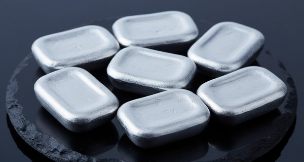 Figure 1: Soft silvery-white high-purity indium ingots with characteristic concave surfaces on dark obsidian
Indium exhibits two stable isotopes: ¹In (4.3%) and ¹In (95.7%), the latter possessing a nuclear spin of 9/2 that finds application in nuclear magnetic resonance studies. For transparent electronics and photovoltaic applications, isotopic composition is not critical, but specialized nuclear and spintronic research may specify isotopically enriched material.
Our indium inventory spans the complete range of physical forms required by researchers and process engineers across the optoelectronics, photovoltaic, and semiconductor industries.
Cast ingots serve as the standard reference form for indium supply, providing feedstock for wire drawing, foil rolling, alloy melting, and precursor synthesis. Each ingot is cast under protective atmosphere and individually certified.
These wrought forms support thermal interface bonding, cryogenic sealing, vacuum gasket fabrication, and experimental electrical interconnect studies. Indium's softness and ductility enable it to conform to irregular surfaces, making it ideal for cold-weld seals in UHV systems.
 Figure 2: Spool of soft silvery-blue indium bonding wire for semiconductor and vacuum applications
Pellet and powder formats provide convenient charging for thermal and electron-beam evaporation, alloy synthesis, and powder metallurgy research. Controlled particle size and surface area ensure reproducible process behavior.
HIP-consolidated indium targets support research into ITO deposition optimization, CIGS absorber layer formation, and novel transparent conducting oxide development. Fine grain structure ensures uniform target erosion and reproducible film properties.
ITO — a solid solution of approximately 90% In₂O₃ and 10% SnO₂ by weight — represents the dominant transparent conducting oxide in commercial use. Deposited as a thin film 50–300 nm thick, ITO achieves sheet resistances below 15 ohms per square while maintaining optical transparencies exceeding 85% in the visible spectrum. This unique combination enables transparent electrodes in LCD, OLED, and plasma displays, capacitive touch panels, electromagnetic interference shielding, and smart window applications. Advanced sputtering techniques have reduced ITO layer thicknesses from 200 nm to sub-100 nm while preserving electrical performance, yielding 30–40% material savings per unit area.
 Figure 3: Circular ITO sputtering target with dark metallic surface mounted in vacuum deposition equipment
Copper indium gallium selenide (CuIn₁₋ₓGaₓSe₂) thin-film solar cells have achieved laboratory efficiencies exceeding 23%, with commercial modules averaging 17–19%. In the CIGS absorber layer, indium contributes the distinctive bandgap and high optical absorption coefficient that enable efficient photon harvesting with film thicknesses below 2 μm. The shift toward perovskite/CIGS tandem architectures, with efficiencies surpassing 30%, is increasing indium layer thickness requirements from 0.5 μm to 1.2 μm per cell. Building-integrated photovoltaics (BIPV) favor lightweight, flexible CIGS modules, with European market growth at approximately 30% annually.
Indium's low melting point and exceptional wetting characteristics on glass, ceramics, and metals make it the basis for solder systems that bond temperature-sensitive components. Indium-tin (52% In, mp 118°C) solders glass and ceramics; indium-silver alloys provide high-reliability electrical connections for aerospace and cryogenic systems; and indium-gallium eutectics remain liquid at room temperature for thermal interface and soft robotics applications. These alloys retain ductility at cryogenic temperatures where conventional solders become brittle, making them essential for superconducting systems and space instrumentation.
 Figure 4: Layered CIGS thin-film solar cell structure showing absorber and transparent conductive layers
Indium phosphide (InP) substrates, grown from high-purity indium, serve as the platform for high-frequency photonic integrated circuits, 5G/6G millimeter-wave devices operating above 28 GHz, and InGaAs detectors for telecommunications and sensing. InP substrates for 6-inch wafers consume approximately 15 kg of indium per 10,000 wafers, and with over 25 million 5G base stations expected by 2028, associated indium demand could reach 400 tons. Our high-purity indium metal provides the consistent feedstock quality necessary for reproducible single-crystal growth and controlled doping profiles.
Pure indium foils and indium-based alloys function as thermal interface materials between high-power semiconductor devices and heat sinks. The metal's softness enables it to fill microscopic surface imperfections, reducing thermal contact resistance by 40–60% compared with conventional thermal pastes. Applications include CPU packaging, power module assembly, LED thermal management, and concentrated photovoltaic cooling systems.
The sensitivity of optoelectronic device performance to trace impurities makes indium purity selection a critical decision. The matrix below provides practical guidance.
| Grade | Characteristics | Recommended For |
| In 4N (99.99%) | Standard optoelectronic; trace metals < 100 ppm | General ITO, thermal interfaces, low-temp solders |
| In 4N5 (99.995%) | Enhanced; Pb, Cd, Sn controlled | OLED electrodes, fine-pitch touchscreens, research |
| In 5N (99.999%) | Semiconductor-grade; total metals < 10 ppm | CIGS solar cells, InP substrates, LED fabrication |
| In 6N (99.9999%) | Ultra-high; GDMS verified ppb levels | MBE source material, quantum devices, standards |
Eata Energy certifies every indium batch through a multi-technique analytical protocol designed to verify purity at the ppb level and ensure suitability for the most demanding applications.
 Figure 5: Ultra-thin reflective indium foil being unwound from a large industrial roll in a clean facility
Research programs and manufacturing process development frequently require indium configurations beyond standard catalog offerings. Eata Energy partners with your technical team to develop bespoke solutions.
Contact our materials engineers during project planning to optimize indium selection for your specific transparent electronics, photovoltaic, or thermal management application.
| Catalog Number | Product Name | Order | Quantity |
|---|---|---|---|
| HPMHPI-0001 | Indium Rod, 99.99999% (7N) | Inquiry | |
| HPM-HPI-0001 | Ultra-High-Purity Indium Continuous Spool Wire | Inquiry | |
| HPMHPI-0002 | Indium Wire, 99.999% (5N) | Inquiry | |
| HPM-HPI-0002 | Ultra-High-Purity Indium Spool Rod, 2 mm | Inquiry | |
| HPMHPI-0003 | Indium Beads, 99.9999% (6N) | Inquiry | |
| HPM-HPI-0003 | High-Purity Indium Pellets and Lumps | Inquiry | |
| HPMHPI-0004 | Indium Sheet, 99.99% (4N) | Inquiry | |
| HPM-HPI-0004 | Light-Tight High-Purity Indium Foil | Inquiry | |
| HPMHPI-0005 | High-Purity Indium Ingot, 99.99999% (7N) | Inquiry | |
| HPM-HPI-0005 | High-Purity Indium Foil, Film and Sheet | Inquiry |
For Research or Industrial Raw Materials, Not For Personal Medical Use!
|
There is no product in your cart. |

Eata Energy is your trusted partner for high-performance energy materials, customized R&D support, and a stable global supply chain. We support you every step of the way in energy innovation.
Enter your E-mail and receive the latest news from us.
Copyright © Eata Energy. All rights reserved.
