
Eata Energy supplies polycrystalline silicon for customers developing photovoltaic materials, semiconductor processes, crystal-growth programs, and advanced silicon products. Our sourcing scope can cover high-purity polysilicon chunks, granular polysilicon, deposited rods, crushed feedstock, selected cast forms, and customer-defined material configurations.
Polycrystalline silicon consists of elemental silicon containing many crystalline regions rather than one continuous single crystal. In the upstream solar and semiconductor supply chain, however, the term most commonly refers to highly purified silicon feedstock produced before single-crystal or multicrystalline ingot growth. It may be delivered as broken chunks, granules or beads, rods, or other charge-ready forms.
This distinction matters when reviewing an inquiry. High-purity polysilicon can be melted to grow monocrystalline ingots by the Czochralski route, or it can be directionally solidified to form multicrystalline ingots. A request for a finished polycrystalline wafer, a cast multicrystalline block, or a high-purity feedstock material therefore involves different specifications and should be identified clearly at the quotation stage.
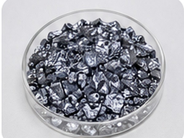 Figure 1. Sized polycrystalline silicon pieces prepared for controlled crucible charging and materials evaluation.
| Product Form | Typical Role | Details to Define |
| Polysilicon chunks | Broken high-purity silicon pieces for crucible charging, remelting, crystal growth, or process development. | Chunk size distribution, fines limit, surface condition, purity profile, packaging, and required documentation. |
| Granular polysilicon | Free-flowing bead or granule form commonly associated with fluidized-bed production and automated or controlled charging. | Granule size, bulk behavior, dust or fines expectations, purity, surface condition, and packaging. |
| Polysilicon rods | Deposited rod material that may be supplied intact, sectioned, or converted into smaller feedstock forms. | Rod dimensions, deposited grade, surface handling, cutting or crushing requirement, and impurity controls. |
| Crushed or sized feedstock | Selected particle range for laboratory melting, pilot trials, charge blending, or specialized processing. | Target minimum and maximum size, oversize and undersize limits, quantity, cleanliness, and packing format. |
| Cast multicrystalline silicon | Directional-solidification material for wafer studies, grain-structure evaluation, machining, or materials research. | Ingot or block geometry, grain characteristics, resistivity, dopant, usable region, cut plan, and inspection requirements. |
| Custom silicon pieces and samples | Discs, blocks, cubes, plates, or irregular samples for analytical work, coating studies, and process trials. | Drawing, dimensions, tolerance, mass, surface preparation, edge condition, cleaning, and individual packaging. |
Two production routes are widely discussed for high-purity polysilicon. In the Siemens process, purified silicon-containing gas is decomposed on heated silicon starter elements, building dense deposits that develop into rods. The rods are removed and can be broken, classified, cleaned, and packed as chunks. This route is associated with established high-purity production for solar and electronic applications.
Fluidized-bed reactor (FBR) production deposits silicon onto small seed particles suspended in a flowing gas stream. As the particles grow, they become dense enough to leave the active bed and are collected as granular polysilicon. Granular material can offer useful flow and charging behavior, but suitability still depends on the required purity, particle distribution, surface condition, and downstream equipment.
Eata Energy does not treat the production route as a stand-alone quality claim. Buyers should connect the route to measurable requirements such as elemental purity, donor and acceptor levels, metallic contamination, carbon and oxygen expectations, particle morphology, surface cleanliness, and batch documentation.
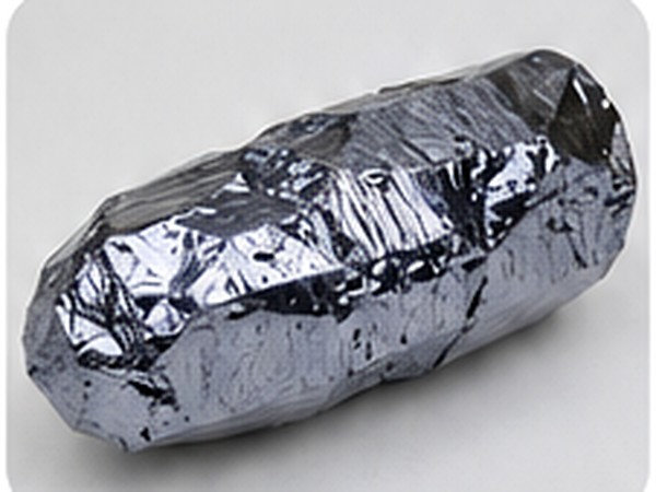 Figure 2. Representative bulk polycrystalline silicon in a rod-like form for downstream sizing or remelting.
The table below is a quotation framework rather than a fixed stock specification. Values and test methods should be confirmed for the selected product because solar-grade, electronic-grade, laboratory, and industrial requirements are not interchangeable.
| Specification Field | Quotation Basis |
| Material identity | Elemental polycrystalline silicon / polysilicon; distinguish feedstock from finished multicrystalline wafers or cast blocks. |
| Grade or intended sector | Solar, semiconductor, crystal growth, laboratory, pilot processing, or another application-defined grade. |
| Product form | Chunk, granular, bead, rod, section, crushed feedstock, ingot, block, plate, or custom piece. |
| Silicon purity | Customer-defined minimum silicon content or grade basis, supported by agreed analytical documentation where available. |
| Dopant-related impurities | Boron, phosphorus, or other electrically active elements controlled according to the intended crystal-growth or device route. |
| Metallic impurities | Selected metals, total metals, or element-by-element limits based on the process sensitivity. |
| Other impurity controls | Carbon, oxygen, chlorine-related residues, or other agreed parameters when relevant to the production route and application. |
| Particle or piece size | Nominal range, maximum dimension, minimum dimension, fines content, oversize allowance, or drawing dimensions. |
| Surface condition | As-produced, crushed, classified, cleaned, etched, or otherwise prepared according to the agreed specification. |
| Morphology and flow | Chunk geometry, granule shape, dust level, packing density, or handling behavior where charging performance matters. |
| Packaging | Clean inner packaging, double-bag format, sealed container, inert option, individual sample protection, or project-specific packing. |
| Inspection and documents | Certificate of analysis, particle-size report, impurity data, lot identification, dimensional inspection, or other agreed records. |
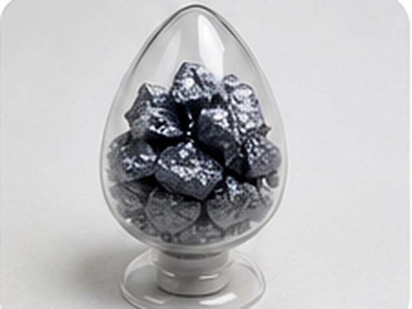 Figure 3. Protected bulk polysilicon sample illustrating contamination-conscious handling.
In a typical crystalline-silicon value chain, high-purity polysilicon is charged into a crucible and melted. For monocrystalline material, a seed crystal is used to draw a single-crystal ingot. For multicrystalline material, controlled cooling and directional solidification allow multiple grains to develop within a cast ingot. The resulting ingot is cropped, squared or shaped, and sliced into wafers for downstream cell or device processing.
Feedstock condition can influence this sequence before crystal growth even begins. Very small particles may affect handling and dust management, while large pieces can influence packing and melting behavior. Surface contamination may enter the melt, and electrically active impurities can alter the properties of the grown crystal. For this reason, a useful purchase specification combines chemistry, geometry, cleanliness, and handling requirements.
 Figure 4. Crystalline-silicon photovoltaic surfaces illustrating a key downstream application.
 Figure 5. Clean industrial process hardware illustrating controlled high-purity material production.
| Decision Point | What to Specify |
| Begin with the downstream process | State whether the material will be melted, directionally solidified, pulled into a single crystal, crushed, analyzed, coated, or machined. |
| Define purity by critical elements | List the impurities that affect the project instead of relying only on a general grade label or number of nines. |
| Match the form to the charging method | Specify chunks, granules, rods, or a particle-size range according to crucible size, automated handling, packing, and melt behavior. |
| Control fines and surface condition | Set expectations for dust, undersize material, cleaning, etching, or as-produced surfaces where contamination or handling is sensitive. |
| Provide dimensional requirements | For blocks, plates, discs, and cut samples, include drawings, tolerances, edge condition, surface finish, and orientation if relevant. |
| Confirm packaging and documentation | Identify clean-pack requirements, individual protection, lot segregation, certificates, impurity reports, and inspection records. |
A headline silicon percentage does not show which impurities are present, how they were measured, or whether the material was handled in a way that protects its surface. For demanding projects, the more useful questions are which analytical method was used, whether values are lot-specific, which elements have individual limits, how particle size is controlled, and what packaging barrier is used after final preparation.
The acceptable specification also depends on scale. A small experimental melt may require carefully sized pieces and detailed analytical data, while a production-scale program may focus on charge behavior, consistency across lots, impurity distribution, and repeatable packaging. Eata Energy can structure the inquiry around the technical risk that matters most to the buyer.
Eata Energy can evaluate customized polycrystalline silicon requirements for research programs, pilot processes, and industrial manufacturing. Possible customization areas include material grade, production route preference, impurity profile, boron and phosphorus limits, metallic-element controls, chunk or granule size, fines allowance, rod or section dimensions, cast block geometry, cutting, crushing, cleaning, sample preparation, packaging, and requested inspection data.
For non-standard items, a technical brief or drawing is the fastest way to avoid ambiguity. Include the intended process, target quantity, critical chemistry, dimensions or particle range, surface requirements, packaging, test methods, and acceptance criteria. Feasibility and the final specification are confirmed against the complete request.
| Catalog Number | Product Name | Order | Quantity |
|---|---|---|---|
| SEM-MSS-0011 | Polysilicon Raw Materials | Inquiry | |
| SEM-MSS-0012 | Photovoltaic-Grade Polysilicon | Inquiry |
For Research or Industrial Raw Materials, Not For Personal Medical Use!
|
There is no product in your cart. |

Eata Energy is your trusted partner for high-performance energy materials, customized R&D support, and a stable global supply chain. We support you every step of the way in energy innovation.
Enter your E-mail and receive the latest news from us.
Copyright © Eata Energy. All rights reserved.
